Rejunity’s Designs
Two designs on this GFMPW-1 submission were contributed by Rejunity. More information on these can be found at these links:
Pinouts
The pinouts of these projects on this particular chip are:
SN76489
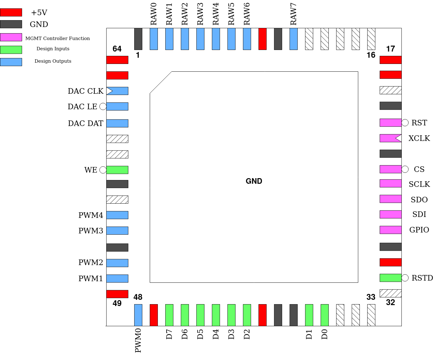
Pin # |
Name |
Type |
Summary |
|---|---|---|---|
|
RSTD |
I |
Active low design reset |
|
D[7:0] |
I |
Data Inputs |
|
PWM[3:0] |
O |
Individual PWM audio output for each channel |
|
PWM4 |
O |
PWM audio output for mixed audio from all channels |
|
WE |
I |
Active low Write Enable |
|
DAC DAT |
O |
Serial Data for external DAC (DAC7611 or similar) |
|
DAC LE |
O |
Active low Latch Enable for external DAC |
|
DAC CLK |
O |
Serial Clock for external DAC |
|
RAW[7:0] |
O |
Raw digital audio sample output with 8-bit resolution |
AY8913
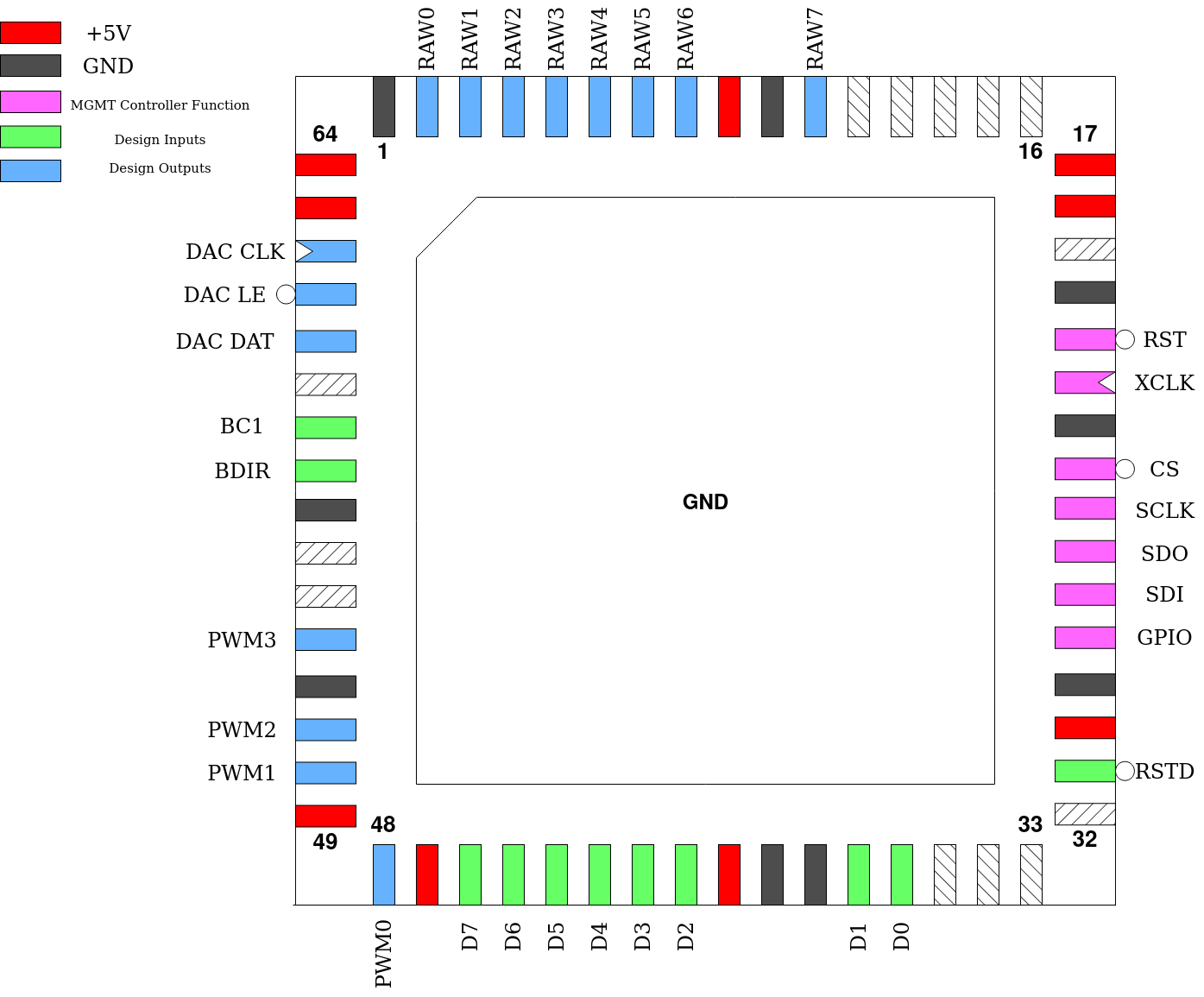
Pin # |
Name |
Type |
Summary |
|---|---|---|---|
|
RSTD |
I |
Active low design reset |
|
D[7:0] |
I |
Data Inputs |
|
PWM[2:0] |
O |
Individual PWM audio output for each channel |
|
PWM4 |
O |
PWM audio output for mixed audio from all channels |
|
BDIR |
I |
Bus control signal |
|
BC1 |
I |
Bus control signal |
|
DAC DAT |
O |
Serial Data for external DAC (DAC7611 or similar) |
|
DAC LE |
O |
Active low Latch Enable for external DAC |
|
DAC CLK |
O |
Serial Clock for external DAC |
|
RAW[7:0] |
O |
Raw digital audio sample output with 8-bit resolution |
Custom Settings
Both designs use the first two bits of reg_mprj_settings to set a clock divider for the whole design.
SN76489
reg_mprj_settings value |
Setting |
|---|---|
0 |
Div by 16 |
1 |
Div by 1 |
2 |
Div by 128 |
AY8913
reg_mprj_settings value |
Setting |
|---|---|
0 |
Div by 8 |
1 |
Div by 1 |
2 |
Div by 128 |