DRAM Controller
This design is a controller for retro DRAM chips that automatically generates RAS and CAS timings as well as regular refresh cycles, simplifying system design. Only two standard 74-series support ICs are required for normal function. The easiest use case is to control 64K DRAMs, but 128K and 256K DRAMs may also be controlled.
The controller is entirely agnostic to the word length of the system, but requires an address space of at least 256 addresses (8-bits) on the side of the host system for configuration purposes. The host system must also support waiting for memory controller operations to complete, as indicated by the RDY/RDYn output.
The input clock to the controller must not necesarily be the same as that of the host system and it is infact recommended to use 2 or 4 times the host system clock, if possible. The only restriction is that CSn, R/Wn and CONFn must be synchronous to the input clock. A PLL (i.e. ICS501) is thus recommended for multiplying the host system’s clock to generate the controller’s clock input.
The typical input clock rate is 33MHz, but any clock rate below this, down to zero is possible as this is a fully static CMOS design.
Pad Assignments
Pad |
Name |
Type |
Summary |
|---|---|---|---|
|
|
I (PD) |
Host address bus input |
|
|
O |
Controller Ready output |
|
|
I |
Active-low design reset |
|
|
I (PD) |
Host address bus input |
|
|
O |
(Debug) Output mirroring the |
|
|
O |
(Debug) Output mirroring the |
|
“Needs Refresh” |
O |
(Debug) Output that is high when a refresh cycle is pending, but has not yet begun |
|
|
I |
Host address bus inputs |
|
|
I (PU) |
Chip Select input |
|
|
I (PU) |
Read/Write select input |
|
|
I (PU) |
Configure select input or host address bus input |
|
|
O |
DRAM Address outputs |
|
|
O |
(Debug) Test output |
|
|
O |
DRAM Address outputs |
|
|
O |
DRAM Row Address Strobe output |
|
|
O |
DRAM Column Address Strobe output |
|
|
O |
DRAM Write Enable output |
|
|
O |
DRAM Address output |
|
|
O |
Data Buffer Enable output |
|
|
O |
Read Latch Clock output |
|
|
O |
Write Latch Clock output |
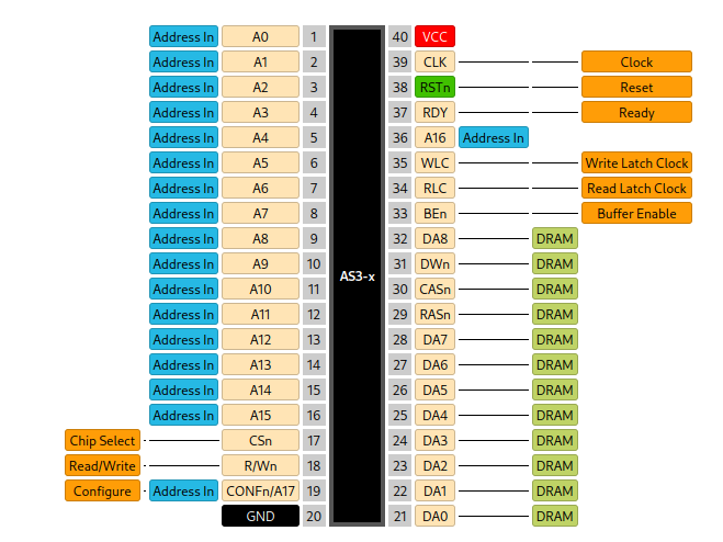
Intended Pinout
The pad-out of this design was carefully selected to allow bonding to DIP-40-compatible COB PCBs or DIP-40 ceramic carriers. The intended pinout is shown below.
Configuration
After reset, the controller first needs to be configured by loading 11 configuration registers. Pulsing CSn and CONFn low at the same time will load these registers sequentially. An internal pointer to these registers is maintained by the DRAM controller and incremented after each use of CONFn, which wraps back to zero after the last register is loaded. All memory requests will be ignored until all configuration registers have been loaded at least once.
Each register is 8-bits wide, but due to the lack of a databus connection to the host system, the A[7:0] address lines are used as the source of data to be copied into the current configuration register. Configuration is thus done by accessing specific memory addresses with CONFn low, with the least significant 8-bits of the address value into the controller being copied into one of the configuration registers.
The configuration registers, in order, are as follows:
This pair or registers sets up rate at which DRAM refresh cycles occur. A refresh cycle is marked as pending every refresh_interval + 1 clock cycles. Note that if this coincides with an ongoing memory access, the controller will finish this access before beginning the refresh cycle.
This register contains various configuration options.
column_bits contains how many of the DRAM address bits are used for the column address minus one. The minimum value is zero (1 column address bit) and the maximum value is 8 (9 column address bits).
rdy_polarity controls the polarity of the RDY/RDYn pin. If zero, RDY/RDYn is active high, if one, RDY/RDYn is active low. The default after reset until this configuration register bit is programmed is active high.
page_mode_en determines if the controller should keep RASn asserted and the current row selected for as long as possible following a memory access. This can save time on subsequent accesses to the same row, but not all memory chips support this. A memory access to a different row or a refresh cycle are causes to de-select the current row and select a new one.
do_data_setup may be set to deal with particularly long data setup times on the DRAM. If set, the controller will wait delay_setup + 1 clock cycles after asserting BEn before continuing.
If delay_rdy is set, the assertion of RDY/RDYn is delayed by one clock cycle if page_mode_en is set, and delayed by delay_ras_precharge + 2 clock cycles if page_mode_en is clear. This is intended to be set when page_mode_en is clear.
Data setup delay to DRAM if do_data_setup is set, don’t care otherwise.
Unused, don’t care.
Delay after falling RASn edge during refresh cycles. The controller will wait delay_ras + 1 clock cycles after asserting RASn when beginning a refresh cycle.
Delay after falling CASn edge during memory access cycles. The controller will wait delay_cas + 1 clock cycles after asserting CASn during a memory access before continuing.
Delay after falling RASn edge to assertion of CASn during memory access cycles. The controller will wait delay_ras_to_cas + 1 clock cycles after asserting RASn during a memory access.
Delay after rising RASn edge to allow for precharge to complete. The controller will wait delay_ras_precharge + 1 clock cycles after deasserting RASn, either in a refresh cycle or memory access.
Delay after rising CASn edge to allow for precharge to complete. The controller will wait delay_cas_precharge + 1 clock cycles after deasserting CASn during a memory access.
This register contains additional configuration options.
configure_enabled determines if the CONFn pin should be disabled. If it is cleared, the controller will stop responding to the CONFn input until a full reset occurs, allowing simple system setups where CONFn and R/Wn are shorted together.¹
¹Errata: Broken. Do not set this bit to zero.
conf_is_a17 allows the CONFn pin to be used as the A17 host address bus pin to address 256K DRAMs on DIP-40 packaged parts. configure_enabled must be set to zero for conf_is_a17 to take effect, but if this is the case, A17 is remapped from its usual pad to that of the former CONFn.²
²Errata: Broken. Also do not set this to one.
If pause_on_refresh is set, RDY/RDYn is deasserted during all refresh cycles, even if no memory request was made by the host system.
Memory access function
To function properly, two support ICs are required, both of which are standard 74HC(T)574s. These form the write and read buffers respectively, buffering the data lines between the host system bus and the DRAM data buses. The simplest possible setup for this is shown below:
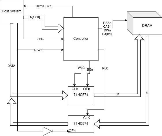
Whenever the controller detects a falling edge on the CSn pin (while CONFn is high) and is not already serving a memory request, it begins either a memory read or write depending on the state of R/Wn. If a refresh cycle is currently in progress, it is completed first before the memory request is served. In any case, RDY/RDYn is deasserted immediately. The controller then performs the necessary row and column address strobes to either write a word of data from the buffers to the DRAM or read a word of data from the DRAM to the buffers. As soon as this is complete, RDY/RDYn is asserted, signaling to the host system that the memory request has completed.
In the case of a read, the read word is held in the read latch indefinitely, allowing the host system to retrieve it at any arbitrary time after the read has completed. In the case of a write, the word to be written is latched, triggered by a pulse on the WLC pin, which occurs on the same clock cycle as RDY/RDYn being deasserted. After this, the host system bus is free to be used for other purposes in the meantime.