AS65RV32
The AS65RV32 is a RISC-V, rv32ima_zicsr_smrnmi processor with some built-in peripherals that is pinout and bus-signaling compatible with either the MOS 6502 or 6510 microprocessors (selectable). It features the same 8-bit databus, but optionally expands the address bus to its full 32-bits. Both NMI and regular interrupt requests function mostly as described in RISC-V specs, but are instead vectored by reading the interrupt handler address from memory in the same way as it is done by the 6502/6510 microprocessors.
Two pad-out configurations are available. Project ID 'b01000 selects the AS65RV32 with 6510-compatible pad-out, including the 6-bit GPIO port, while 'b01001 selects the AS65RV32 with 6502-compatible pad-out.
Special note: this design is clocked on the falling edge of the input clock signal.
Pad Assignments
Pad |
Name |
Type |
Summary |
|---|---|---|---|
|
|
I (PU) |
When low, forcefully tri-states the address and data buses as well as the |
|
|
O |
Indicates that a read-modify-write cycle is in progress (i.e. atomic instruction) |
|
Disable write pauses |
I (PU) |
Changes the behavior of the |
|
Half write cycle |
I (PU) |
When high, the data bus is only an output for half a clock period on write cycles, instead of a full clock period, as in the original 6502/6510 processors |
|
TXD |
O |
Transmit line of the built-in UART |
|
|
I (PU) |
A low level on this input sets the |
|
|
O |
Phi2 clock output (inverse of input clock) |
|
|
I |
Active-low reset input |
|
|
I |
Input that, while low, pauses the processor during a memory access, forcing it to wait for slower memory |
|
|
O |
Phi1 clock output if the |
|
|
I |
Low-level-sensitive external interrupt input |
|
|
O |
Address Latch Enable output which pulses high when the high-order address bits are presented on |
|
|
I |
Non-maskable interrupt trigger, falling-edge triggered |
|
|
O |
Status output indicating that the current bus cycle is an instruction fetch in-progress |
|
|
I (PU) |
Receive line of the built-in UART |
|
|
O |
Address bus outputs, multiplexed in extended bus mode |
|
Sync |
I (PU) |
If high, the |
|
|
O |
Part of the address bus outputs |
|
No Connect |
NC |
Unused |
|
|
O |
Part of the address bus outputs |
|
|
IO |
Bi-directional data bus (note reversed bit order compared to pad numbering) |
|
|
O |
Indicates if the current bus cycle is a read (high) or a write (low) |
Pad |
Name |
Type |
Summary |
|---|---|---|---|
|
|
IO |
Bi-directional data bus |
|
|
IO |
Bi-directional data bus |
|
|
O |
Indicates if the current bus cycle is a read (high) or a write (low) |
|
|
O |
Phi1 clock output |
|
|
I |
Active-low reset input |
|
Half write cycle |
I (PU) |
When high, the data bus is only an output for half a clock period on write cycles, instead of a full clock period, as in the original 6502/6510 processors |
|
TXD |
O |
Transmit line of the built-in UART |
|
Disable write pauses |
I (PU) |
Changes the behavior of the |
|
|
I (PU) |
Receive line of the built-in UART |
|
|
I |
Input that, while low, pauses the processor during a memory access, forcing it to wait for slower memory |
|
|
I |
Low-level-sensitive external interrupt input |
|
|
I |
Non-maskable interrupt trigger, falling-edge triggered |
|
|
I (PU) |
When low, forcefully tri-states the address and data buses as well as the |
|
|
O |
Address bus outputs, multiplexed in extended bus mode |
|
Sync |
I (PU) |
If high, the |
|
|
O |
Part of the address bus outputs |
|
|
IO (PU) |
GPIO port bit 5 if |
|
|
IO |
GPIO port bit 4 if |
|
|
IO |
Bits 1 through 3 of the GPIO port |
|
|
IO |
Address Latch Enable output if in extended bus mode, GPIO port bit 0 otherwise |
|
|
IO |
Bi-directional data bus |
¹This pin acts as RXD after reset. However, while reset is active, on every falling clock edge, its state (high or low) is latched and used as another configuration option: “Sync IRQs”. If low upon reset being released, the IRQn and NMIn inputs are henceforth internally buffered through latches on every falling clock edge.
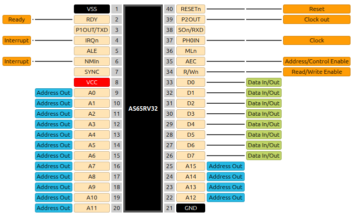
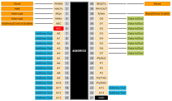
Intended Pinouts
The pad-out of this design was carefully selected to allow bonding to DIP-40-compatible COB PCBs or DIP-40 ceramic carriers. The intended pinouts are shown below. Just how the project selection pins are intended to be selectively bonded to the ground plane inside the package, the various configuration pins (such as bidir[27] on either pad-out option) are also pulled high by default and may be bonded to ground selectively.
DIP-40 Pinout for 6502 pad-out
DIP-40 Pinout for 6510 pad-out
Bus Interface
Basic Bus Cycle
Effect of “Half write cycle” low
Successive writes
The R/Wn pin remains low for successive writes and does not pulse for each byte. Only address and data change on the falling edge of the clock.
Reset/Vector Fetch Sequence
After reset goes high, the CPU starts up in non-extended bus mode, with only 16-bit addresses. However, to ensure hardware intended for extended bus mode starts up correctly, a single pulse is emitted on ALE with the address lines set to 'hFFFF to initialize the address latches.
On the 6510-compatible pinout, where all P[5:0] pins are intended to be in a high-impedance state after reset, this means pin P0 will briefly become an output, emit the pulse, then return to its high-impedance state. A pull-down resistor on this pin is required if it is to be used as ALE after initialization and a series resistor is required if it is to be used as a general-purpose input in non-extended bus mode.
After this pulse, the processor performs a vector fetch, whereby four successive bytes are fetched starting at address 'hFFFC and then loaded into the Program Counter before beginning program execution. These vector fetch cycles are identical when an interrupt looks up its vector, but using different addresses.
Peripherals
GPIO Port
The 6510-compatible pad-out offers a 6-bit GPIO port with individually programmable port directions. It is accessed through the following non-standard CSRs:
ddr - Data Direction Register - 'hBC0
port - Port Register - 'hBC1
The bits in ddr set the direction of the GPIO pins: a one sets that pin to an output while a zero sets that port to a high-impedance input. Writing port will then set the high or low state of all pins configured as output while reading port returns a mix of the current output states of the output pins and the current input levels of the input pins.
Note that relocating the UART overrides these settings for port bits 5 and 4, and switching to extended bus mode overrides the setting for port bit 0. Controlling the direction and value of these pins then no longer is possible through these CSRs.
UART
Both pad-out variants provide pads for a UART serial port. By default, the receive and transmit lines for this port are allocated to pads which are not otherwise used. However, these pads are not exposed on the DIP-40 pinouts. To allow the UART to be exposed on the DIP-40 pinout without potentially breaking backwards-compatibility with existing pin functions, the UART can be relocated by setting the uart_reloc bit in the cpuconf CSR. Doing this switches two pins on the DIP-40 pinout to become the new RXD and TXD. Note that, if this is done, the UART continues to transmit on both the non-relocated and relocated TXD.
The UART is usable through the following non-standard CSRs:
ustat/utx - UART Status - 'h139
This CSR reads 'hFFFFFFFF if the UART transmitter is busy and no new characters can be sent right now. Otherwise, if the transmitter is idle, it reads zero.
If written to, the least-significant 8 bits of the written value are captured and sent to the UART transmitter to be serially transmitted on TXD. The transmitter enters the busy state until transmission is complete.
urx - UART Receive - 'h140
If read, this CSR reads the current 8-bit, zero-padded value in the UART receive buffer, if one is available. If the receive buffer is empty, it reads 'hFFFFFFFF. Reading this register clears the receive buffer.
udiv - UART Clock Divisor - 'h142
This CSR defines the amount by which the processor clock is divided to arrive at the UART bitclock. The UART bitclock will be equal to CPU clock / (UDIV + 1). Upon reset, its value is set to 88, which approximately equals a 115200 bitrate at an input clock of 10MHz.
Interrupt-capable timer
A single 32-bit presetable timer allows for generation of regular interrupts on the processor. The timer will count up from zero until it reaches or exceeds the value defined in itimermatch, at which point it will reset to zero and also generate a regular interrupt if the corresponding interrupt enable is set.
The timer value can be read out and set at any time by accessing its CSR. As such, it is also possible to use it as a general-purpose timer under software control.
The following non-standard CSRs control timer operation:
itimer - Timer value - 'hBC3
itimermatch - Timer compare match - 'BC4
Pseudo-RNG
A LFSR-based PRNG is constantly being updated at every clock edge and its current value can be read from this non-standard CSR:
rng - PRNG value - 'hFC7
Standard CSRs
Name |
Address |
Contents |
|---|---|---|
|
|
Zero |
|
|
|
|
|
Zero |
|
|
|
|
|
|
|
|
Clock cycles since reset - LSBs |
|
|
Clock cycles since reset - MSBs |
|
|
Clock cycles since reset - LSBs |
|
|
Clock cycles since reset - MSBs |
|
|
Retired instructions since reset - LSBs |
|
|
Retired instructions since reset - MSBs |
¹Errata: this value is invalid as it specifies MXL == 1, when it should be zero.
²Errata: ebreak instructions are counted in instret, even though they are not supposed to be.
cpuconf CSR
A non-standard CSR called cpuconf exists to configure the operation of the AS65RV32. It contains three bits. In order, these are:
uart_reloc: setting this moves the UART TXD and RXD pins to alternate locations.
O: general-purpose flag that can be arbitrarily set and reset. It provides compatibility for the SOn pin found on the original 6502. A low level on SOn sets the O flag. If the UART is relocated or the 6510 pad-out option is used, this flag is not affected by any pad inputs.
bus_extend: setting this switches the CPU to extended bus mode, where a full 32-bit memory address is multiplexed onto the A pins via ALE. On the 6510 pad-out option, this disables one of the GPIO port bits. When bus_extend is cleared, all memory addresses leaving the CPU are truncated to 16-bits. Note that this immediately sends out a pulse on ALE at the start of the first instruction fetch after bus_extend is set, to sync the most-significant bits of the Program Counter.
All bits in this CSR are zero after reset.
cpuconf - CPU Configuration - 'hBC2
Interrupts / Traps
Interrupts on the AS65RV32 are mostly compliant with RISC-V specs, except for the fact that they fetch the vector addresses from main memory, rather than CSRs. When an interrupt is handled, the CPU first reads 4 bytes from a specific memory address and copies this word into the Program Counter, before resuming execution. The following locations are used:
Source |
Address |
|---|---|
Reset |
|
Regular Interrupt |
|
Non-Maskable Interrupt |
|
Reserved |
|
For regular interrupts, the CSRs mcause, mscratch, mie, mip, mepc, mstatus and mstatush are present, as well as the mret and wfi instructions.
As only two asynchronous sources of interrupts exist (IRQn pin and timer interrupt), only the relevant bits are implemented, i.e. meie and mtie in mie, with the rest hard-wired to zero.
CSR |
Bits |
|---|---|
|
|
|
|
|
|
|
|
The mcause CSR contains one of three values according to the source of the interrupt:
Source |
Value |
|---|---|
|
|
Timer interrupt |
|
Breakpoint |
|
The breakpoint interrupt is caused immediately by execution of a ebreak 3 instruction, no matter the current interrupt enable status.
If multiple interrupts are pending concurrently, they are served according to this priority (most significant first): Breakpoint -> Timer -> IRQn pin.
Non-Maskable Interrupt
The non-maskable, negative edge sensitive interrupt pin, NMIn, functions mostly according to the Smrnmi RISC-V spec, with the exception that its vector is fetched from main memory, as described in the previous section. For NMIs, the CSRs mncause, mnscratch, mnepc and mnstatus are present, as well as the mnret instruction.
mncause always reads 'h80000000 and only the bit NMIE is implemented in mnstatus. All other bits are hard-wired to zero.