Commodore 64 PLA
This design is a replica of the PLA chip used in the Commodore 64 home computer, but implemented through discrete logic rather than an actual PLA. Implementing this circuit in a way that does not cause timing problems with other chips inside the Commodore 64 requires specific input-to-output propagation delays to be met. As this delay was difficult to estimate for this multi-project die, several different delay lengths are selectable through the CASDEL[1:0] and DEL inputs. The former selects a delay specifically for the CASRAMn output, while the latter selects the delay for all other outputs. All of these inputs have built-in pull-ups, meaning any delay can be selected by hardwiring or bonding specific inputs to ground.
When DEL is high, it selects additional delay. Otherwise, no additional delay is added.
CASDEL[1:0] features four possible delay settings:
|
Setting |
|---|---|
|
Short delay |
|
Medium delay |
|
No delay |
|
High delay |
Pad Assignments
PLA Pin descriptions taken from the C64 wiki.
All unused pads should be hardwired or bonded to ground, if possible.
Pad |
Name |
Type |
Summary |
|---|---|---|---|
|
|
I |
Connected to R/#W of the bus |
|
|
I |
#AEC, connected to inverted version of AEC on the VIC-II |
|
|
I |
Connected to BA on the VIC-II |
|
|
I |
Connected to A12 of the address bus |
|
|
I |
Used for programming field-programmable parts and not connected internally for mask programmable parts. |
|
|
I |
Connected to A13 of the address bus |
|
|
I |
Connected to A14 of the address bus |
|
|
I |
Connected to A15 of the address bus |
|
|
I |
Connected to #VA14 on VIC-II |
|
|
I |
Connected to #CHAREN on I/O port of the 6510 CPU |
|
|
I |
Connected to #HIRAM on I/O port of the 6510 CPU |
|
|
I |
Connected to #LORAM on I/O port of the 6510 CPU |
|
|
I |
Connected to #CAS on the VIC-II |
|
|
O |
#ROMH |
|
|
O |
#ROML |
|
|
O |
#I/O |
|
|
O |
GR/#W, connected to #WE on the color RAM |
|
|
O |
Connected to #CS1 on the #CHAROM |
|
|
O |
Connected to #CS on the #KERNAL ROM |
|
|
O |
Connected to #CS on the #BASIC ROM |
|
|
O |
#CASRAM, connected to the #CAS pin on the DRAM |
|
|
I |
Chip Enable / Output Enable (active-low) |
|
|
I |
Connected to VA12 on VIC-II |
|
|
I |
Connected to VA13 on VIC-II |
|
|
I (PU) |
Delay select for all outputs except |
|
|
I (PU) |
Delay select for the |
|
|
I |
Connected to #GAME on pin 8 of cartridge port |
|
|
I |
Connected #EXROM on pin 9 of cartridge port |
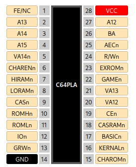
Intended Pinout
The pad-out of this design was carefully selected to allow bonding to DIP-28-compatible COB PCBs or DIP-28 ceramic carriers to form a drop-in replacement for the Commodore 64 PLA chip. The intended pinout is shown below.